
PAGE CONTENTS
Objectives
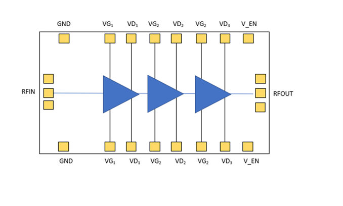
The AmpliKa project aims to develop a high-efficiency Ka-band MMIC chipset in a Wafer Level Chip Scale Package (WLCSP) format, featuring a Variable Gain Amplifier (VGA), Power Amplifier (PA), and Low Noise Amplifier (LNA). This format offers advantages in cost, size, weight, and power over traditional packages, targeting high-frequency beamforming antenna systems for satellite and terrestrial communications. Applications include satellite and ground communications, as well as beamforming antenna arrays that may require hundreds to thousands of chipsets. Suitable WLCSP packaging will be evaluated, assessing flip-chip and Land Grid Array (LGA) options. A primary objective is to qualify the reliability of this packaging format for space use, advancing its technology readiness level (TRL) from TRL3 to TRL5.
Challenges
- Thermal management: High power output amplifiers generate significant heat, requiring advanced cooling techniques to prevent degradation.
- Efficiency optimisation: Balancing high efficiency and linearity, especially for Power Amplifiers, to avoid excessive power consumption.
- Frequency precision: Ensuring consistent performance across specified frequencies (17.7-30 GHz) requires tight control over design parameters.
- Noise minimisation: Achieving <2.2dB noise in the LNA while maintaining gain is challenging, demanding careful material and architecture choices.
- VGA linearity: Ensuring efficient linear performance across the VGA’s gain range (5-20dB) without signal distortion.
- Integration: Compactly integrating multiple functionalities on a single chip for space-limited designs.
System Architecture


Plan
Definition stage
- Define complete product requirements and initial design for feasibility and risk mitigation.
- Mid-Term Review milestone.
- Establish baseline design for the technology phase.
- Preliminary Design Review milestone.
Technology stage
- Develop an initial breadboard chipset for component/process qualification; conduct thermal, RF, and mechanical testing.
- Assess breadboard and qualify improvements.
- Critical Design Review milestone.
- Create Engineering version of chipset (Dev 2) for further qualification.
- Qualification Test Review milestone.
- Test engineering version with industry partners for verification at MMIC LAB.
Current Status
The project kick-off meeting was held on 7 November 2024. The Mid-Term-Review will occur on 3 March 2025.
Companies