
PAGE CONTENTS
Objectives
The objective of the project is to build an optical receiver for high-speed free-space optical (FSO) communications which combines the two functions of 1) data receiver and 2) optical beam tracker in a single detector. It is based on a specifically developed high-speed, low noise, long wavelength avalanche photodiode together with commercially available electronics. An evaluation board is developed as part of the project, containing all the input/output connectors needed to easily test the receiver functionalities in a laboratory environment.
The primary application of the receiver is in the Optical Ground Stations (OGS) used for LEO direct-to-Earth connections. However, given the similarity of the requirements, the receiver developed here could be also used for inter-satellite and terrestrial FSO communications. FSO links transmit information from point to point using a narrow beam of light. This type of networks is becoming more and more widespread because of some unique advantages compared to conventional radio frequency wireless networks and fibre connections. These include immunity to spectrum congestion and interference, improved security, lower power consumption and rapid deployment in difficult-to-reach areas.
Benefits
The role of the product in the context of the overall system/service of its target users is to combine the two functions of tracking sensor and data receiver to improve sensitivity and reduce cost and complexity in optical ground stations for high-speed satellite-to-ground optical links. Any FSO data link between satellites and the ground requires a constant adjustment of the receiver orientation, in order to track the signal from the fast-moving satellite in orbit. This is normally accomplished by employing an optical system where the light beam is collected by a telescope and split in two branches: one is sent to a segmented detector, the other to a fast receiver. The detector is connected to the beam steering system of mirrors, and is used to track the light source and maximize the amount of light collected onto the receiver, which actually detects the data stream. The product under development in this activity combines these two functions in a single device. This brings several key advantages:
-
Improved data sensitivity;
-
Reduced material budget, simplifying its integration into satellites;
-
Reduced complexity of the optical system;
-
Higher data rate compared to existing solutions, up to ≥10 Gbps.
Features
The core of the receiver is a four-quadrant avalanche photodiode chip. This is a photodiode where the active region sensitive to light is divided into four independent segments. The chip has an effective light-collecting area of at least 200 µm diameter. The chip sub-assembly is then incorporated in a hermetic package together with individual transimpedance amplifiers (TIAs), limiting amplifiers (LIAs) and passive electrical components (capacitors, resistors, inductors…). The precise package form factor definition is covered as part of the project. The receiver is designed to be suitable for different data rates, including 100 Mb/s, 1.5 Gb/s and ≥10 Gb/s, with a dedicated filter for each data rate. The operation wavelength is 1550 nm.
Challenges
Main challenge of AO-RETINA project is to find an optimum balance between the high data rate for data receiving and the large light sensitive area for beam tracking.
Main technical requirements are the following:
-
Multiplied responsivity > 9.0 A/W at 1550 nm;
-
High data rate operation up to 10 Gbps;
-
Low noise multiplication to obtain high sensitivity operation;
-
At least four independent segments for beam tracking with total detecting diameter of 200 µm.
System Architecture
The following product tree is a hierarchical breakdown of the product into the hardware and software elements:
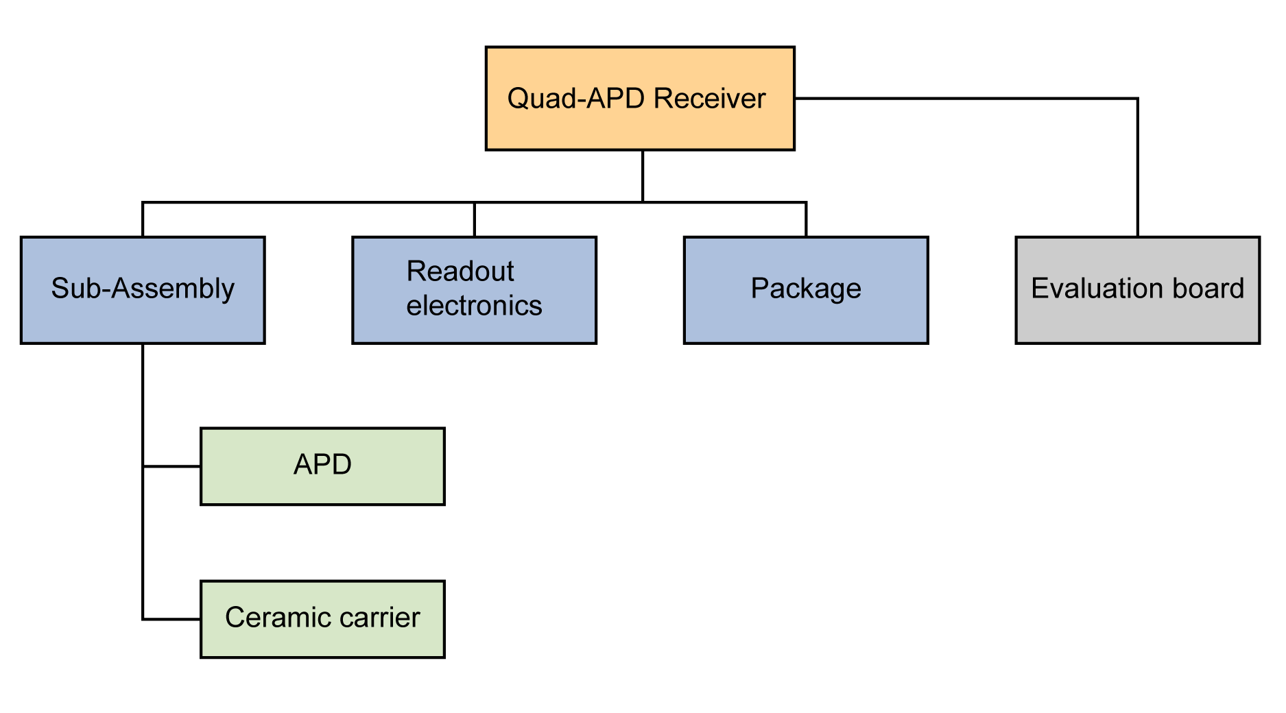
The key products or elements are described below:
APD chip
The APD chip detects the optical signal, both for beam tracking and for data transmission purposes. The chip translates the optical input into an electrical output. Thanks to the avalanche multiplication process in the APD, the chip offers an internal gain, allowing the detection of very low power optical signals. In order to be able to track the beam position, the chip is divided into four or more segments with independent anode and cathode contacts for individual readout. The chip backside features an integrated lens which helps to collect the light and focus it to the active region(s).
Readout Electronics
The circuit amplifies the RF electrical signal produced by the APD and provides individual outputs from each quadrant, as well as a sum data output. If required, it can also provide a discretized digital signal (hard decision “0” or “1”).
Evaluation Board
The purpose of the board is to allow an easy evaluation of the receiver performance, offering all the required connections for biasing and signal readout.
Plan
The technology development of this project is divided into two phases: a “Technology – preparation” phase and a “Technology – development” phase. In the preparation phase, we cover the following tasks: conducting literature research to review the state of the art, preparing the device design, and running simulations. In the development phase, we design and measure tests to validate the simulation models, verify compliance with project requirements, and define the final design. The final design is then manufactured and tested.
Current Status
The project has been started with a Kick-Off-Meeting in May 2023. The project is currently in the “Technology – preparation” phase.
Our team has concluded an assessment of the current advancements in the field of the tracking and data transfer receivers and currently undergoing a deep dive into the development of the simulation models. Albis team is actively engaged in brainstorming sessions to create an innovative and optimal device design that can accommodate the demanding technical requirements of AO-RETINA project.
Related Links
Companies
