
PAGE CONTENTS
Objectives
The project’s goal was to develop electro-photonic building blocks for next-generation telecommunication payloads, focusing on frequency downconversion between feeder and user links in future Q/V band communications. The EPFCV2 photonic chip performs downconversion from the Q/V band (up to 50 GHz) to the Ka band (around 30 GHz), designed to be frequency-agnostic for multiple applications. This allows integration into Very High Throughput Satellites (VHTS) targeting 1TB/s data rates. The device leverages the advantages of photonic-enabled payloads, including reduced mass, power consumption, and cost, while enhancing flexibility and capacity.
The new satellite payload concept requires numerous feeds or phased array systems, which involve many converters and stable clock distribution. Additionally, laser communication for inter-satellite links is emerging as a secure, high-data-rate solution, beneficial for fleet operations. This technology has been recently demonstrated for GEO-LEO relay, LEO constellations, and lunar communication. The project consortium includes Antwerp Space (AS) as the prime contractor, Fraunhofer HHI institute as the photonic integrated circuit (PIC) foundry partner, and Alter UK for packaging the PIC
Benefits
1. Cost reduction. Notably through:
-
Mass reduction on the frequency conversion section of the payload. Further harness mass reduction, pending replacement of low power waveguides or even coaxial cables above Ku band by optical fibre. This directly affects the payload launch and maintenance cost.
-
A reduction in the payload integration time, due to replacement of low power waveguides by optical fibre.
-
Optical fiber allows tight and flexible bending and more compact routing network inside the satellite.
2. Reliability increase, thanks to:
-
An overall simplification of the architecture of the payload’s frequency conversion section. This in turn would generate a reduction in the number of points of failure.
-
All photonics elements are insensitive to electromagnetic interference (EMI) and do not generate EMI.
-
Transmission loss in the optical domain is much lower using optical fiber (0.2 dB/km).
-
Better phase stability of the optical routing over temperature and when is bended in comparison with coaxial cables
3. High throughput, thanks to:
-
Broadband modulation bandwidth is provided by photonic devices up to 10 Gb/s using simple NRZ-OOK modulation.
-
Possibility of low loss and high data-rate multiplexed signal routing for multi-functional optical payload (switching, RF filter, delay line, etc.)


Features
EPFCV2 integrates in a single platform a frequency agnostic device that can be configured to carry out one of three tasks: Frequency conversion, Photonic Local Oscillator distribution and data-optical transducers for intersatellite links. Photonic integration technology offers high bandwidth elements that can work up to the Q band with RF losses significantly lower than the traditional microwave counterpart. Additionally, since the photonic building blocks are intrinsically broadband, the same photonic chip can be allocated to operate in any frequency band as long as it is within the operating bandwidth of the chip. In this case the photonic chip could operate between DC to 50 GHz. Furthermore, on the same chip, the transmitter, a laser and a high bandwidth IQ modulator were hosted. On the other chip, the receiver, an optical amplifier and a high bandwidth photodiode were integrated. These two pioneering combinations of photonic building blocks offer high power efficiency and low noise operation.
Challenges
The project aimed to deliver a high bandwidth, low noise and power efficient frequency downconverter based on integrated photonic technology. The first challenge was to integrate on the same chip a high frequency I-Q modulator, a laser source and on a second chip a high bandwidth photodiode and a semiconductor optical amplifier. When the project started, these devices (modulators, lasers) were realized in separate chips. Integrating them in the same chip enabled a more efficient device, the manufacturing of a device with such level of integration was a pioneering work. An additional challenge was the development of efficient driving electronics for the PIC.
System Architecture
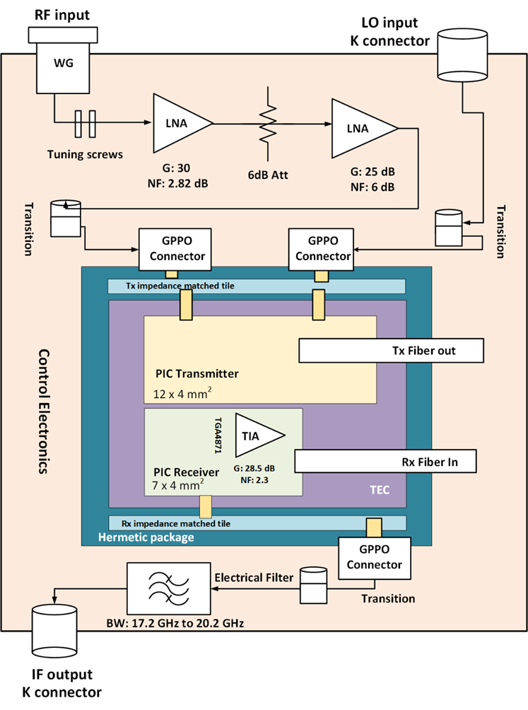
The system architecture is detailed in the figure. The equipment is comprised of an RF board, a control board and the packaged photonic circuits. The RF board deals with the inputs, Rf signal and Local oscillator (LO) and the intermediate frequency (IF) output. The PPIC hosts two PICs: a transmitter and a receiver. The transmitter encodes the RF signal and the Lo in a light beam. The light signal is couple into an optical fibre leaving the equipment. The optical signal can be distributed into the spacecraft with significantly lower losses and ease of routing than a coaxial cable. The PIC receiver converts the optical signal back to the electrical domain into a downmixed IF.
Plan
The project milestones were: System Requirement review, where the needs of the space sector in terms of functionality and performance were analysed and translated into requirements for the photonic IC, the packaging, the RF and control boards. Then the best possible technological platform had been selected in the next milestone, Technology Selection Review. The work was then split in three, HHI was in charge of the PIC development, Alter of integration and packaging and Antwerp Space took over the system engineering tasks, development of electrical boards and project management. Once the pieces of hardware had been manufactured an integrated, they could be tested.
Current Status
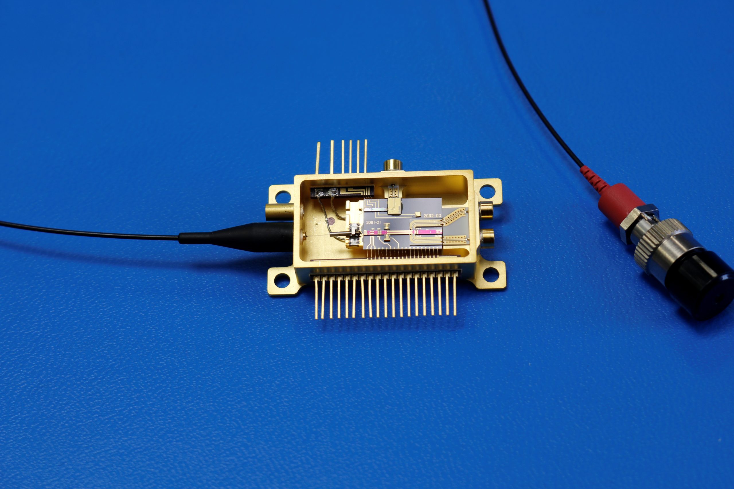
The project has been completed and a Demonstrator has been realized. Several challenging and pioneering activities have been accomplished. The development of RF interposers with a 50 GHz bandwidth for packaging, high frequency electro-optic interfaces have been realized. On the Integrated photonic side, a very innovative chip has been manufactured, with the co-integration of building blocks that were not integrated before on the same chip. Leading to a strong improvement in the manufacturing process.