PAGE CONTENTS
Objectives
The project objectives are as follows:
-
To determine which compound semiconductor process, from the available commercial MMIC foundries, is most suitable for the next generation of Ka-band power amplifiers. These will be used in GIL satellite ground terminals. Comparing measured and foundry data the preferred process was selected based upon simulated data in a 2.5W PA baseline design.
-
The selected process, GaN-on-Si process, D01GH was subsequently to be used in a MMIC class BJF-1 PA design. The overall amplifier performance is to be determined by simulation.
-
Three commercially available amplifiers were measured in a suitable test fixture and PCB to determine which best meets the GIL specification. Target powers were taken as 2.5W and 4W across the Ka band. From these measurements one MMIC is selected to be incorporated in a package and mounted on a dedicated transceiver board to be tested in a GIL XRJ transceiver housing and a limited lifetime test undertaken.
-
The resulting measurements were used to update the PA specification and ultimately the Business Case for next generation GIL satellite ground station transceivers.

Challenges
The key technical challenges of the project were:
-
to secure foundry samples to enable an informed choice of process for the PA design exercise.
-
The design challenge was for the amplifier topology, class BJF-1, to achieve the bandwidth, power and efficiency for a viable MMIC.
-
Achieving good performance of the selected MMIC in the chosen Kyocera package, with designed alumina inserts and on a dedicated PCB in the GIL XRJ transceiver housing.
The prime management challenge was to complete the project through the disruption of the COVID pandemic and with significant personnel changes.
System Architecture
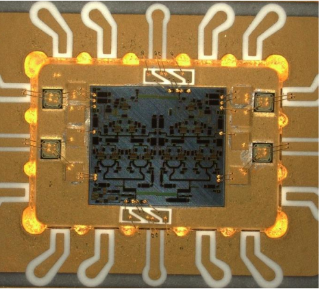
The proposed system architecture for the XRJ transceiver is to take the nominated Iconic ICP2840 die and package that in a Kyocera SGMR-A2416-B RF package. The Kyocera package is relatively inexpensive and has good thermal performance for heatsinking. There is also the space in package to accommodate decoupling chip capacitors in package that help stabilise the device and alumina tiles performing compensation matching at the RF input and RF output for the die in package. The package, die and components are then epoxied into the package and gold-wire bonded. The whole package is then mounted on a purpose designed PCB on the low loss substrate Rogers 4003C LoPro PCB and built into Global Invacom’s cutting edge Ka-band VSAT XRJ transceiver test housing which has a waveguide port to the antenna.
If the University of Sheffield MMIC design was subsequently fabricated, the packaging and PCB would be redesigned to accommodate the smaller and possibly cheaper die.
Plan
This project had 3 major milestones; these were to design a Ka-band MMIC PA suitable for the use in the XRJ transceiver. The foundry process to be used was determined by sample assessments from WIN and OMMIC foundries. In parallel, three commercially available die were sourced, mounted on test fixtures and measured for power, bandwidth, linearity and efficiency. Of these three candidates one, the Iconic ICP2840, was selected for mounting in a package and on a suitable modified PCB for testing the XRJ housing. Tests were taken of two units. The business plans were subsequently updated.
Current Status
The project deliverables have been achieved with the design of a Ka Band PA MMIC with P1dB >36dBm and efficiency 25 – 31% across the band 27.5 – 31GHz on the OMMIC D01GH GaN-on-Si process. This amplifier uses the novel class BJF-1 to achieve 3% higher efficiency than a standard class AB design would yield.
In parallel, three candidate off-the-shelf MMICs were tested in fixture and against the targeted specification and the Iconic ICP2840 selected for testing in the GIL XRJ transceiver housing. Generally, performance was good and in a limited lifetime test power degraded by only 0.4dB.
Companies

